PHYSICAL LAYER #04
Semiconductor Equipment
Metrology, Precision Thinning & Advanced Bonding
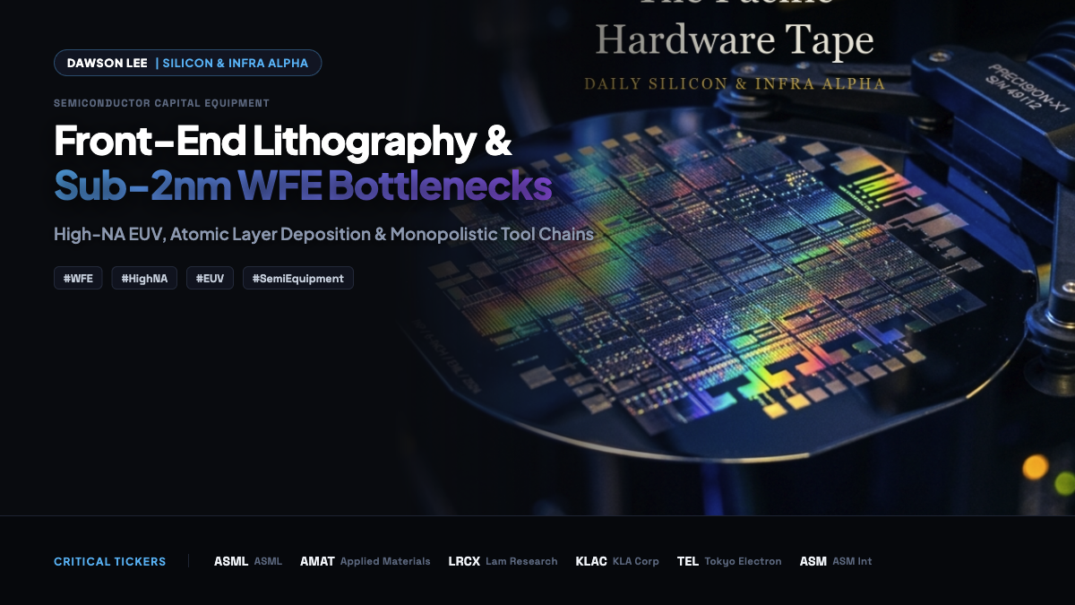
PHYSICAL BLUEPRINT • LAYER #04 SEMICONDUCTOR EQUIPMENT
Key Research Question:
“How much does inspection and metrology value density expand as multi-die package cost exceeds $10,000 per module?”
30µm Wafer Thinning TTV Limits & TC Bonder Throughput
Key Technologies in this Layer
Ultra-Thin GrindingTC BonderHigh-Pressure AnnealingEUV Metrology